Introduction
Nvidia launched the 900 series this September, as usual starting with their “flagship” GTX 980 and the slightly cut down GTX 970. With the 980 priced at $549 and the GTX 970 priced at $329 and with both cards featuring sub 200W TDPs, the VGA market was drastically changed in a single day. Although Nvidia has been cutting down the power consumptions of their cards continuously since the infamous GTX 480 BBQ edition, Maxwell has really redefined the power to performance ratio at a time where AMD is concurrently struggling to cool their R9-290x cards.
Nvidia gave us a taste of Maxwell back in February of last year when they launched the awesome 750 Ti. The reference design of the 750 Ti features a ridiculous TDP of 55W and doesn’t even require a single 6 pin. Although it wasn’t part of the 900 series and wasn’t the flagship card, it got enthusiasts craving for more Maxwell because it performed so well (at such low power) for such a low end card. Now with the 900 series Nvidia has continued with their low power trend.

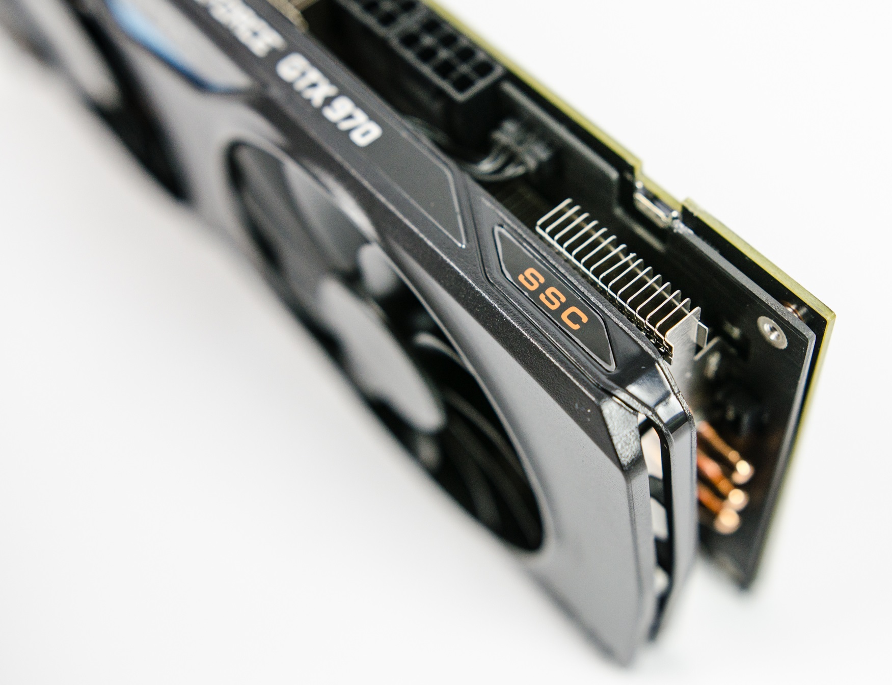
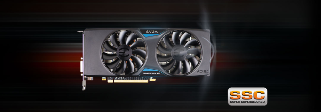
Despite the impressive power consumption numbers, neither GPU is lacking in processing power. While our GTX 980, GTX960 SSC, and Titan X reviews coming in the near future, we were thoroughly impressed by the performance from it’s little brother, the GTX 970. EVGA provided our sample today, their EVGA GeForce GTX 970 SSC ACX 2.0+. As usual, EVGA is currently offering no less than eight different SKUs ranging from $329.99 to $389.99.
Unlike the GTX 980, Nvidia didn’t initially offer a reference board with their classic cooler that the GTX 980 sports. Currently Nvidia only offers what some may consider a reference design with classic cooler exclusively through Best Buy for $379.99 – however it’s important to point out that the PCB is actually more similar to that of a GTX 980, even being compatible with GTX 980 water blocks. Since no reference design was made available, GPU vendors were given the ability to choose which PCB they wanted to use. While this helped Nvidia’s partners clear out old PCBs, it rubbed some people the wrong way, particularly those that like to water cool. With no reference design, end users had to be very careful when choosing which card they were going to go with if they wanted to water cool. Manufacturers used PCBs from the very dated 660 Ti all the way to the brand new GTX 980. While EVGA is using their own custom GTX 760 solution for their 970s, it’s very similar for the entire lineup, which allows water cooling manufacturers to create a single block for all cards. Luckily this meant that many of the old waterblock designs were later found to be compatible with various 970 designs.
Below you will find tables for all of the higher end AMD & Nvidia GPUs from the past couple of years. Keep in mind that all cores are not created equal! CUDA Cores =/= Stream Processors performance wise, even Kepler Cores =/= Maxwell Cores. Let’s start with AMD:

As with the Kepler GTX 680 and 780 generation Nvidia decided to save the highest end Maxwell version for later, first launching with the Titan X before trickling down to unnamed GTX models later. The GTX970 is therefore not based on the high end GM200 core but the “midrange” GM204 chip. This is the same chip as in the GTX 980 but with some cores disabled.

Now that you’re caught up on the technical part of the GPU, lets take a look at this specific model!





[…] […]
Comments are closed.