


Since the launch of AMD’s multi die ThreadRipper, there has been some confusion about how this particular CPU works. So we decided to start a new series where we explain new tech and how it works.
Die configuration
First off – what do we mean by a “die”? Processors are usually made out of billions of CMOS transistors created on a large silicon crystal that has been sliced into thin discs called wafers. Ions are fired through masks to “dope” areas of silicon both positively and negatively to create the transistor structures. These transistors are then connected with many metal layers above the silicon. Once all the layers have been built up which can take months of manufacturing time then the wafer can be cut up into the individual “dies”. So essentially most processors would have one die, or simplistically one lump of intricately manipulated silicon. Now you can’t just plug silicon directly into a motherboard, it needs to be put into a protective package that also allows all the connections to reliably and easily mated with the motherboard. Most basic chips would use a plastic package with metal legs that get soldered down to a PCB. These metal legs get wired to the silicon with tiny “bondwires” inside the plastic package. However CPU’s have gotten far more complex and often have the die itself sit on a mini PCB because the number of pins is so large – take for example Intel’s socket 2011 which has 2011 pins to connect. The bonus of using a mini PCB means that extra components can be mounted to the PCB such as decoupling capacitors that combat power supply voltage droop under load. Now because the CPU needs cooling there needs to be a stable and strong thermally conductive surface on to which to mount a cooler. Both Intel and AMD now use an Integrated Heat Spread or IHS. This is a piece of aluminum that sits on top of the pcb and protects the fragile silicon from damage while transferring heat to the cooler and spreading it out across the whole area of the IHS.
So let’s take a look at the die configuration on ThreadRipper which is rather unique. Unlike most chips which only use one die, AMD have chosen to put four dies on the mini PCB. The dies are the blackish rectangles in the centre of the green PCB:
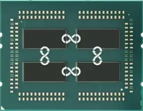
However unlike EPYC two of the dies are disabled and are just there to better support the IHS so it doesn’t sag. Presumably they will also poorly transfer any heat from the PCB substrate also.
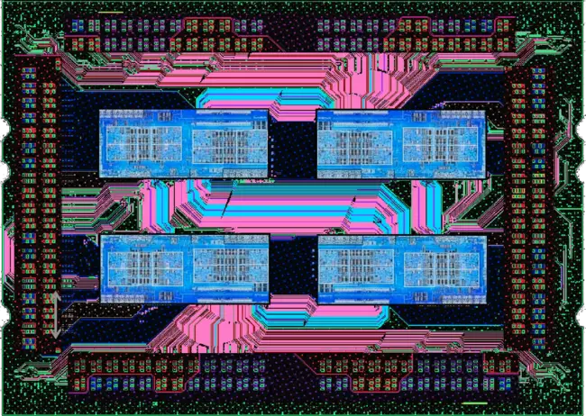
This image is showing the internal metal routing of the PCB with the four dies having massive bus connections between them which AMD have marketed as “Infinity Fabric” in Pink, Blue and Green.
The number of dies used is two, which means with each die being up to 8 cores that the configuration can provide 16 cores at maximum per threadripper CPU. Also each diehas a dual channel memory controller so with two dies, it ends up with quad-channel memory, allowing for potentially higher bandwidth than dual channel alone. However efficiency of this memory bus for a single core may not be as high as for a single die solution with a quad channel memory bus like Intel’s HEDT offerings.
Why do something so complex?
There have been many solutions to upping the core count in these “core wars”. When chips are manufactured there is a certain risk of errors in manufacturing. There manufacturing errors can be tiny, but can make an entire chip unusable. The larger the processor area then the higher the chance of an error within that area. Imagine each wafer has 10 errors. If that entire wafer was 10 chips, then you might not get any good chips. However if that wafer was 100, then you should get at least 90 chips. So large chips have a lower manufacturing yield than smaller chips. Low yield means high price, which is one reason to justify why Intel’s 18 core CPUs that use a single die are so expensive. So at some point it becomes inefficient to just make a massive CPU with a single die.
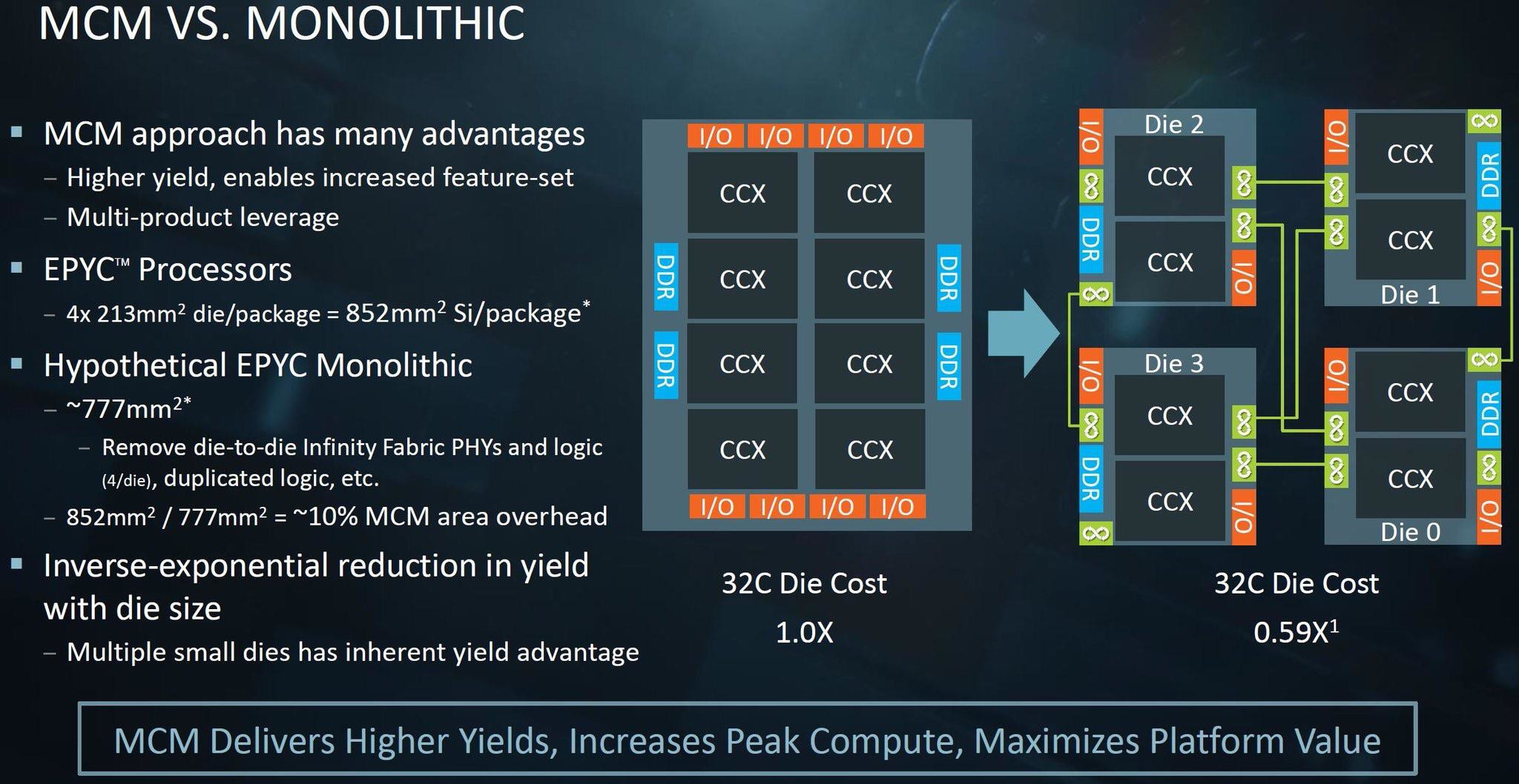
Here is a marketing slide calculation where cost is reduced by 41% which is huge. This is a slide made for EPYC, but it also applies to ThreadRipper.
So the cost efficient solution then is to use multiple dies. Intel and AMD have typically in the past chosen to just use multiple CPUs and connect them on the motherboard with buses. This means more expensive motherboards and slow interconnect buses between the individual CPUs. Threadripper essentially integrates all of this onto the CPU package.
Infinity Fabric:
Infinity Fabric is AMD’s marketing term for the bus connection that connects the processor dies.
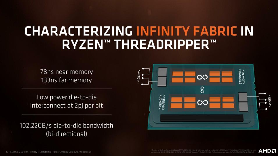
CPU sockets constrain bus speed for two reasons. The socket itself add a lot of capacitance that slows down the maximum signal speed. The buses need to run a fairly long distance between the CPU sockets. They also limit the width of the bus because each data signal in the bus needs at least 1 (often 2 or more) connectors on the socket. By connecting the dies with shorter distances, wider buses and without big slow sockets then the connecting bus can be made faster and more efficient (lower power). The infinity fabric bus runs at 102.22GB/s speed which allows dies to talk to each other without a problem. It also makes reduces the latency for sharing the memory and cache from each core to the other.
So why doesn’t Intel do this? Intel have already chosen the more expensive solution of putting 18 cores on one die. If Intel wanted to put two of those 18 core dies in one massive CPU of course they could. but the problem would be cooling. Both threadripper and the massive core count Intel CPUs are realistically thermally limited from what they could really achieve. You can see that because in real use the maximum single core speed is more than the speed when all cores are working.
So lastly we’ve mentioned EPYC and how similar the setup is to Threadripper. EPYC is the server CPU lineup and so Threadripper is just a modified EPYC CPU with two disabled CPUs. Everything else is same. It uses a similar socket too. The SP3r2(TR4) and SP3 sockets both have the same pin count, 4094, but are not compatible with each other. This is done in order to separate server and consumer parts and their respective price points. So why is cooling a problem for Threadripper and not EPYC? Server parts value power efficiency and so that usually means more cores at a lower speed. Threadripper is designed to not really compromise on single core speed. As EPYC’s speed is lower than Threadripper, power is lower and so you can have more cores for a given thermal power limit.
Closing Thoughts
AMD really offered the market something different with ThreadRipper. Because of it’s cost efficiency advantage it can be priced at “only” $600-1000 which gives it a huge advantage over Intel. Intel may have a slight speed advantage because of it’s “simpler” solution but at almost double the price, it certainly doesn’t offer double the performance.
Still confused – just ask us any question in the comments!


Nice summary. Good post.
Comments are closed.